Cue the Theremin music!
This article is about building your own all-FET Circlotron. It smashes atoms.
No, strike that. It won’t smash atoms like a cyclotron, but it has a really cool name and it is, technically speaking, powered by atoms and very, very good at amplifying music.
Alpha M. Wiggins of Electro-Voice is generally recognized as the inventor of the Circlotron amplifier although other inventors developed similar circuits around the same time period in the 1950’s. The Circlotron’s transformer-coupled vacuum tube output circuit, a floating bridge, was often drawn in a circular fashion; hence the name. Later, Circlotron-type output stages were used to directly couple the output tubes to the loudspeaker and eliminate the need for an output transformer. At one time, Circlotron was an Electro-Voice (EV) trademark, but a cursory trademark search revealed that the name is no longer trademarked, and today the name Circlotron is applied to just about any amplifier with a floating bridge output stage. If you’re a history buff, you may want to check out the “Circlotron History Page”.

Circlotron circuits make for lots of interesting discussion among the audio crowd. They are sometimes thought to posses mystical powers and perform hitherto impossible quantum mechanical wonders. Oftentimes they’re just confusing. More often than not, the discussion turns to intellectual property. A number of patents for Circlotron variants have been issued in the U.S. and many of them deal with biasing arrangements, voltage amplification stages, offset correction, and, and so on. Some of them are pretty novel. In any case, they make for great marketing.
This article describes the design and construction of a fairly straightforward, simple Class A floating bridge amplifier, aka Circlotron. I hope, especially if you are new to this hobby, that you’ll find this project simple and complete enough to actually build, even if it’s your first.
The Floating Bridge
I use the terms “Floating Bridge” and “Circlotron” interchangeably and I believe that “Floating Bridge” more accurately describes the topology and makes for less hocus-pocus. And, since we’re on the subject, let’s start with the output stage and work our way in.
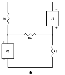
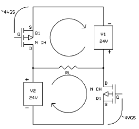
Figure 1a shows a bridge circuit with fixed voltage sources V1 and V2, resistors R1 and R2, and a load, RL. If V1 = V2 and R1 = R2 the bridge is balanced and no current flows through RL. If we change the value of R1, or R2, the bridge becomes unbalanced and a corresponding current flows through RL.
You may already be familiar with bridge circuits used to determine the value of unknown resistances, and you could think of the circuit in Figure 1 as a variation of the classic Wheatstone bridge. If, for example, we know the values of V1, V2, and R1, we could experimentally determine the value of an unknown R2, by measuring the direction and magnitude of the current through RL.
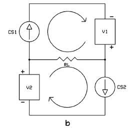
Notice that none of the arms of the bridge is attached to ground. The bridge is floating. Without a load, the circuit forms a single current path. With RL in place, two new current loops are created and that’s where the magic comes in. If you will agree that the resistors approximate current sources, then we can replace the resistors with ideal current sources as in Figure 1b to make our mesh current analysis a snap.
Figure 2
Let’s use 1 Amp for each of the current sources. Once again, if CS1 = CS2 and V1 = V2, the bridge will be balanced and no current flows through the load resistor.
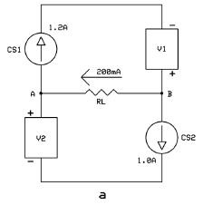
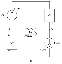
But, f we raise CS1 to 1.2 Amps as in figure 2a, the bridge becomes unbalanced and 200mA is conducted through RL in the direction of the arrow. Alternately, we can raise the value of CS2, and current will flow through RL in the opposite direction as shown in figure 2b.
So, we can push, or we can pull.
Now things are getting a little more interesting, and although we’ve limited the discussion to direct current so far, we might imagine controlling something like a speaker with this arrangement, if only we had a device that would control a large current based on some sort of input signal, maybe even music. Fortunately for us, we have the transistor.
We can replace CS1 and CS2 with transistors which are handy for amplifying audio signals. For this project we’ll use N-channel MOSFETs as seen in Figure 3. The ability to use like-polarity devices in a push-pull arrangement like this is particularly useful in the tube world, where Pchannel tubes don’t exist, but it can also be useful in solid state circuits since not all transistors have exact complements.
For a great explanation of using MOSFETs, check out the Nelson Pass article, “F5 Power Amplifier for PassDIY” on the First Watt website. For now, it’s enough to say that a MOSFET can be used to control a current based on the voltage applied between its gate and source.
Figure 3
Bias
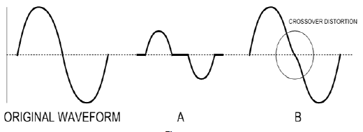
We’re building a push-pull amplifier where the output devices will work in opposition, each handling 180 degrees of our signal waveform. To get our MOSFETs conducting this waveform, we need 3-4 volts between the gate and source pins to turn them on. If we use the input signal alone to supply this voltage, nothing will happen while the signal level is below the turn-on voltage for the MOSFET, and the first few volts of input won’t even show up at our output terminals. It isn’t pretty. See FIGURE 4a. The on and off switching of our transistors can clearly be seen. When the output transistors are only switched on for 180 degrees of the wave cycle we’re operating in Class B; anything less is Class C and neither will do for us.
Figure 4
It would be better to have our MOSFETs a little bit “on” all the time, standing-by to conduct our signals and this is Class AB operation. With this class of operation, we improve our situation, and get the first few volts of our signal back by supplying some DC voltage to turn on our MOSFET and get some current flowing through our output stage. This is called the bias current and it flows all the time, even when there’s no signal. Our bias current could be just a few milliamps, and this might be good in terms of efficiency, but we will see distortion caused by the imperfect transition between output transistors. Figure 4b shows what happens to our output signal. That squiggle in the crossover region (you guessed it) is crossover distortion.
The higher we set the bias, the lower the crossover distortion. If we really want to minimize the crossover distortion, we’ll need to set our DC bias around one-half the peak required output current. This is Class A operation, and it’s good.
Although our amplifier could be operated in any of these classes with varying degrees of success, we will operate it in Class A for the best possible performance.
How much bias current will we need? This amplifier will be conservatively rated for 20 Watts @ 8 Ohms in Class A, so our peak output current will be 2.24A (1.414 * SQRT(20/8). So, we’ll need to set the bias for each output MOSFET around one-half of this value, and we’ll round it up to 1.2A DC.
For 1.2A, we’ll need around 4V DC between the gates and sources of our output MOSFETs and the easiest way to set to set this up is to tap a little voltage from V1 and V2.
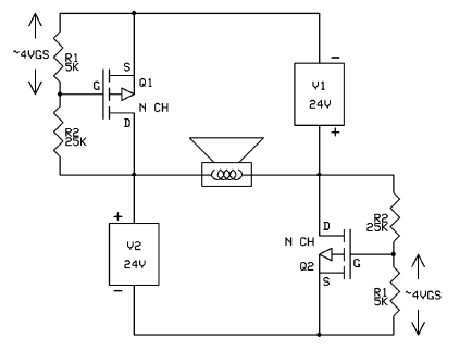
Figure 5
Figure 5 shows the addition of R1, R2. These resistors form voltage dividers. The voltage across R1 is equal to V1 x (R1/(R1+R2)). In this case 4 volts, and that’s about what we want. Now Q1 and Q2 are forward biased and will conduct about 1.2A each. In reality, the current conducted versus the applied gate-to-source voltage varies from part number to part number and from MOSFET to MOSFET, so we’ll need a way to adjust this voltage, or Vgs.
Now that we’ve set up some DC operating parameters for our amp, you may be concerned that your speaker will object to these DC voltages. However, remember if the current through Q1 is equal to the current through Q2, the bridge is balanced and no DC flows through RL. Slight differences between these currents will affect the differential DC offset, which is the DC our speaker will see, and we’ll want to set it to a very small value.
Drive
This is a push-pull amplifier. In a complementary arrangement, one having both N and P type devices, we could drive this output stage with an unbalanced signal where one output device conducts as the signal goes positive and the other conducts as the signal goes negative. But our output stage uses devices of like polarity and, in the case of N channel types; they’ll want to be driven positively from gate to source. This means we’ll need two copies of our signal, one that is positive for the first 180 degrees and another that is positive for the second 180 degrees. Fortunately, a balanced signal provides just what we’re looking for: two copies of our signal 180 degrees out of phase. We could use a transformer or a phase splitter to provide this signal, but for this project we’ll let our balanced preamp or DAC do the job. Please note this amplifier can’t be driven by shorting one of the inputs to ground – not effectively anyway.
Input Stage
We could stop here, add a passive input network and some capacitors for signal coupling to Figure 5, but our amplifier would have slightly less than unity gain, and the bias will wander with our power supply noise, which will find its way to the speaker. I’ve built the amplifier this way, and it worked, but what I really wanted was a little gain, less noise, and a higher input impedance, without adding more power supplies or using transformers.
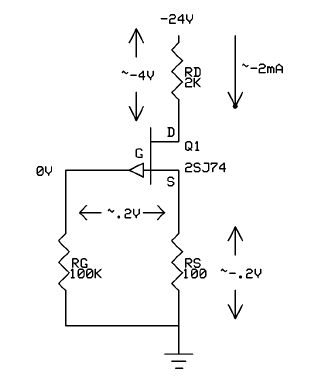
The answer came thanks to the tutorial in the Nelson Pass “F5 Power Amplifier for PassDIY” article. Figure 6 shows a JFET common source amplifier. The circuit has DC coupling, a high input impedance, some gain, and the current flowing through Rd can be used to provide a steady DC voltage to bias our output MOSFET. Sweeeeet!
Figure 6
Complete Channel Schematic
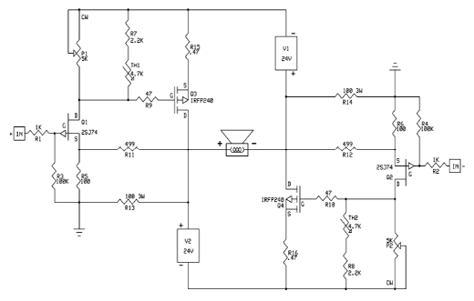
FIGURE 7 is the schematic for a complete channel. We’ve added some source resistors (R15 and R16) to our MOSFET output stage which is driven by two identical JFET common source amplifiers. The 2SJ74BL P-channel JFETs are biased at around 2mA with 100 Ohm source resistors (R5 and R6) which put the gates at 0V DC.
Figure 7
The JFET drain resistors have been replaced by potentiometers (P1 and P2) which allow us to adjust the gate to source voltage of MOSFETS Q3 and Q4.
These adjustment pots are in parallel with R7/R8 and TH1/TH2 which provide a bit of temperature compensation for the output MOSFETs. They help facilitate a faster warm up and lower the possibility of thermal runaway. I consider them a must for this project, and their values are somewhat critical. I learned this the hard way. If you omit them, you should use higher values for R15 and R16, or accept the risk of “China Syndrome”.
R11 and R12 provide feedback and set the gain around 15 dB.
R13 and R14 form a virtual ground for the output and help to stabilize offset drift. They lower the output terminals to around .2 V, and the speaker doesn’t see this absolute DC.
That’s all there is to it: just a handful of parts.
Building and Adjustment
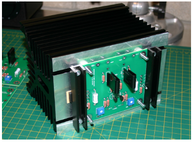
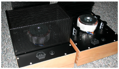
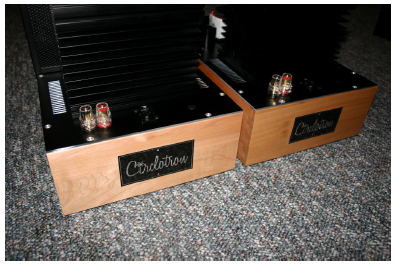
If you want to build a pair of amps just like the ones in the picture, I have included a supplement to this article which details their construction. The construction guide is available as a PDF download from the publisher’s website. The construction method employed is especially good for beginners without machine shops in their basements (The machine shop will come later, friends. You’ve been warned. This hobby has that effect). It includes parts lists, sources, some instructions, and pictures. It’s the next best thing to a kit, and I think they’re sort of retro-cool.
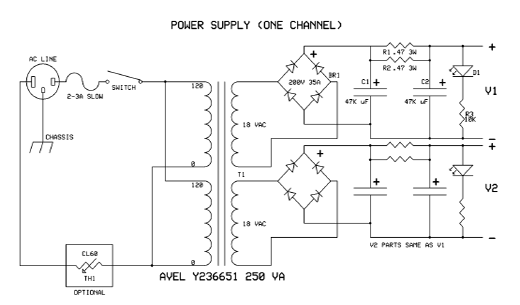
The power supplies for this amplifier are independent and floating! Do not attach any of the power supply terminals to ground. That would be bad. Only the mains earth from the IEC connector is attached to the chassis. You need a separate supply for V1 and V2 and since we’re building two mono channels, we’ll need four supplies. Each pair of supplies can be powered from a single transformer having two independent secondary windings, and many toroidal types are made this way. FIGURE 8 shows a suitable supply for one channel. You can use normal capacitor reservoirs (without the Pi filter) of say 60-100,000 uF which will yield slightly higher, but acceptable, noise figures. If you build the amp according to the construction supplement, the blue LEDs are mounted to the supply PCBs which mount underneath the top plate and give off a nice vacuum-tubey glow from within. I know it’s gimmicky, but this is “The Amazing FET Circlotron”!
Figure 8
After you’ve built and tested the power supplies, assemble and attach the amp channels. Don’t forget V1+ and V2+ are cross-connected. This is very important. Each channel’s heat sink will need to dissipate 60W at no more than 25°C above room temperature.
The signal ground is important. A faulty connection here might upset the bias and cause things to get hot fast, so check for a good electrical connection. Check for continuity back to the earth tab on the IEC connector. Attach it to the chassis right on top of the mains earth lug. If your chassis is anodized or painted, scrape or sand this area to bare metal.
Now it’s time to fire them up. Turn P1 and P2 to their minimum positions (fully CCW if you’re using the PCBs from the construction guide). Be absolutely sure they are at their minimum settings or you run the risk of destroying the output transistors, which will bring the fun to a screeching halt.
Ideally, you should have three multitesters for this procedure (the twenty-dollar kind should work fine. Don’t go crazy.) Use one each to measure current through the output stage, and one to measure the DC offset at the output.
Install a 2-3 Amp slow blow fuse, stand back, and bring the amp up slowly with a variable AC transformer, if you have one. I wear a full face shield and keep a fire extinguisher handy for this. Seriously, in this hobby, things can go pop, melt, and even catch fire, and it often happens at this stage of the game. If you’re not familiar with electrical safety in general, do get familiar. There are articles, videos, and classes available online, through your local community college, or possibly your power company.
Slowly adjust P1 and P2 upward and observe the voltage across R15 and R16. It is easiest to adjust them alternately in small increments of 1/10th of a turn to keep them in balance. You’ll want to measure about 560 mV across each source resistor which corresponds to 1.2A bias. As you approach the target voltages, watch the DC offset meter and adjust the balance for low DC. I found it pretty easy to achieve < 10 mV offset. When the currents are equal, the offset should be near zero, but the lowest offset might be achieved with slightly imbalanced currents. For now, focus mainly on getting the offset low and definitely less than 50 mV.
You’ll need to readjust the bias after a few hours when the heat sink is fully warmed-up, and repeated adjustments may be needed to get everything just right. It’s helpful to put your chassis cover on between adjustments to keep the JFETs close to their normal operating temperatures.
When that’s done, you’re ready to try it out.
What Could Go Wrong?
I must warn you that there are some things that can go wrong. Firstly, this amp has bridge connected outputs, and if one side of the bridge fails your speaker will see some DC; maybe too much. This would most likely result from losing one of your power rails. This is common to many bridged amps, and some have special protection, and some don’t. I just check my power connections really well when I’m building and then I don’t worry about it.
Also, this amp can deliver a hefty amount of current. It doesn’t include any sort of current limiting, so if you decide to short the output terminals you might smell some smoke. This means you must take care in making your speaker connections, and always connect your cables and interconnects with the power switched off.
Measurements
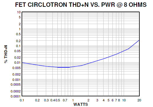
Figure 9 shows the distortion vs. power for an 8 Ohm load. We’re around .005% at one Watt and .2% at twenty Watts.
Figure 9
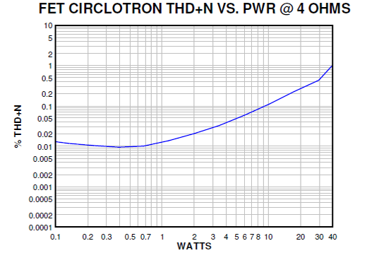
Figure 10 shows the distortion vs. power for a 4 Ohm load, and here we’re around .01% at one Watt and 1% at forty Watts.
Figure 10
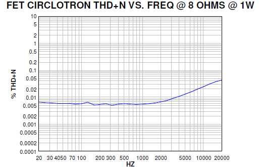
Figure 11 shows the distortion vs. frequency at one Watt into 8 Ohms. Here we see a fairly flat characteristic out to 1 kHz where the distortion begins to rise with frequency.
Figure 11
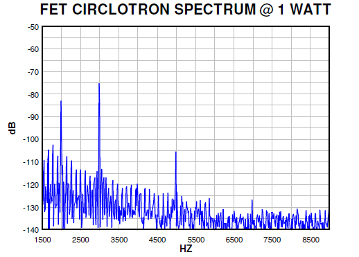
Figure 12 shows the FFT at one Watt. The dominant 3rd harmonic can be seen here.
Figure 12
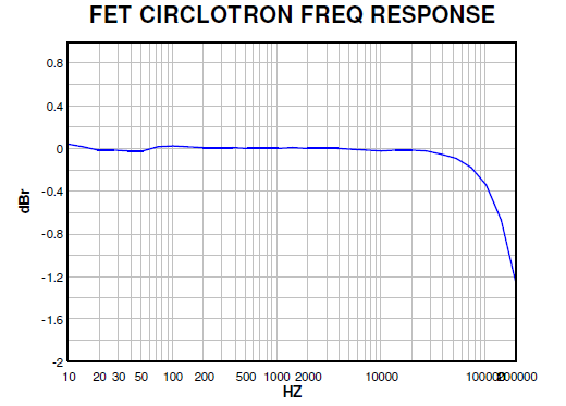
Figure 11 is our frequency response, down 1.5 db at 200 kHz.
Figure 13
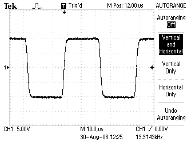
Lastly, figure 14 shows our 20 kHz square wave response.
Figure 14
Tweaking
Our amp’s measured performance is pretty good, and this is with more or less randomly selected parts.
This circuit, as you might expect, will benefit from good symmetry, and a little effort matching parts will pay off. So, what parts should we match? Well, everything if you can. Match your JFETs for Idss and your MOSFETS for Vgs. If you’re lucky enough to score some dualmonolithic 2SJ109BL JFETs, that’d be the cat’s pajamas.
It’s a good idea to have Q1 and Q2 in thermal contact, and you can accomplish this by pressing them together or gluing a small heat sink across their tops.
If you decide to match your resistors, some of the values are low and you might need to use a 4- wire measuring technique to get good matches. In the prototypes, I did try to match-up R13 and R14 since they’re 5% parts. Other than that, things just got plugged in as they came out of their packages.
For R13 and R14, you could substitute the nice TO-220 Caddock power resistors which are noninductive and have a 1% tolerance. I also tried installing a 5K pot across R13 and R14 with the wiper to ground. With this setup, I could dial-in the circuit balance and adjust it for the lowest distortion, but I really didn’t need it with the Caddocks. If you like tweaking, go for it. Otherwise, just build and it and don’t worry so much.
Conclusion
These amps measure pretty well, and are fairly easy to build and adjust. Once you’ve gathered all the parts you can build them in a weekend or two. I’m driving mine with a Pass X2 preamp and I’ve also tried them driven directly from the balanced outputs of a Benchmark DAC-1. Both worked great, and just about any DIY or commercial balanced preamp (tube or transistor) should work just fine.
Now, you’re probably wondering how they sound.
We’ll, first I have to tell you that nothing sounds as good as something you’ve built yourself, and I’m no Dick Oshler when it comes to describing the sound of components.
Having said that, I’ll tell you that they sound great, exhibiting many of the qualities audiophiles crave. Build a pair for yourself. I don’t think you’ll be disappointed. You may even think they’re “Amazing”.
I have a blog at www.audiohobby.com, where I’ll try to post some of the trivial bits that didn’t fit in this article (sort of like the out-take reel). You can contact me there, and I’d really enjoy seeing pictures of your completed amps.
My Quest for Fun
Writing this article has been a personal quest for me. I got hooked on the audio hobby while I was serving in the U.S. Army a long time ago. When I joined, I wanted to be an electronics technician, but color-blindness made that impossible. The Army has funny rules. So, I pursued electronics as a hobby. The first (complete) thing I built was a Pass A40, and I’ve been building stuff ever since.
If you’re just getting started in this hobby, you should know that building audio gear usually leads to tweaking, and tweaking may eventually lead to designing. This is my attempt to do just that. I am truly an amateur in the sense that I have a pretty normal day job, but more in the sense that my electronics education is limited to Ohm’s Law, what I’ve learned by experimenting, and most importantly what I’ve learned from the dozens of articles by Nelson Pass. I know I’ve dropped his name several times in my article, and the truth is - I just can’t thank the guy enough for making this hobby fun.
Now go build something!
Less...


