The Zen Amp concept is an exploration of how well you can make a simple audio amplifier perform. It makes for an interesting illustration of design technique, since more complex circuits are inevitably composed of collections of simple circuits, and it is well recognized that the optimization of these simple sub circuits is usually the key to getting the most out of the larger circuit.
Apart from that, there is aesthetic pleasure in rendering a device in a simple way. Also we find that, other things being roughly equal, simple circuits sound better musically. The Zen series has so far demonstrated that single gain stage amplifiers have enough stand-alone performance to justify their use in audiophile applications. There is no reason why we can’t go on from here to build two and three gain stage circuits, but we have not yet exhausted the possibilities for single gain stage amplifiers, and so we will explore some more.
Complementary Design
Previously we have limited ourselves to single-ended Class A amplifiers, but it’s time to try a complementary (push-pull) design. Since this is supposed to be a tutorial series, we need to ask the primary question, “What
is meant by complementary operation and why do I want it?”
If there is only one gain device, there cannot be complementary operation. If there are two gain devices you can operate them in opposition, one of them conducting more current while the other one conducts less current and vice versa. While this still constitutes one gain stage, the two devices give more gain and
power, and in addition certain types of distortion (principally second harmonic) tend to cancel.
The reason for distortion in an amplifier is pretty much the variation of gain of the active devices over their operating curve. As a transistor or tube experiences greater and lesser voltage and current over the audio waveform it’s gain changes, creating distortion. If an oppositely
operated device has the same sort of character but is operated in reverse, the distortions of the two devices tend to cancel each other out, and you get better performance. This effect is useful, although it is largely limited to second harmonic (non-symmetric), and does not help out at all on odd order (symmetric) distortions.
Technically the Son of Zen project is a complementary stage by virtue of having two single-ended stages, one on each side of the loudspeaker. This has been occasionally referred to as a “balanced single-ended” amplifier, and isn’t what we normally think of when we refer to a pushpull amplifier. However it does benefit from the same distortion cancellation mentioned above, and its character is partly the result of the complementary operation of the transistors.
Common Drain Operation
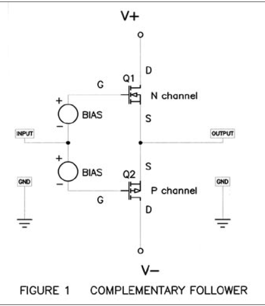
Routinely, designers create singlestage complementary voltage follower amplifiers by using devices of opposite polarity types with both a plus and a minus supply voltage as seen in Fig 1, where two Mosfets can be seen operating in “Common Drain” mode, where the signal goes in the Gate and comes out the Source. The circuit has current gain, but not voltage gain, and is similar to many of the output stages of ordinary multi-stage amplifiers in which a previous stage has done all the voltage amplifying you need.
It operates by having the Source pins of the Mosfets connected to the output, where they tend to follow the voltage presented to the Gates. A bias voltage is

required between the input of the amplifier and the Gates of the Mosfets in order to put the Gates of the Mosfets in the proper DC position. A Mosfet requires about 3 to 4 volts DC between the Gate and Source before it will start conducting, and by adding this to the input, we avoid losing the first 3 or 4 volts of the input signal.
For driving loudspeakers, we usually want the amplifier to have both voltage and current gain. It is a rare preamplifier that will output
the full voltage needed, and this leaves the follower circuit of Figure 1 useful only in a limited number of cases.
Common Source Operation
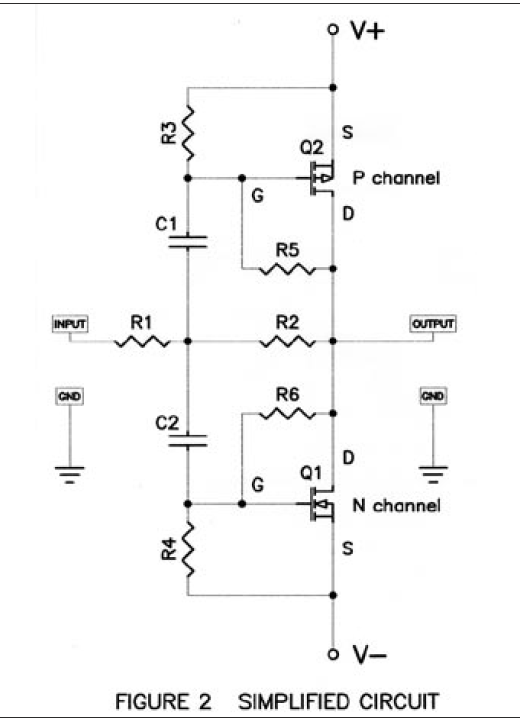
To get both voltage and current gain, the amplifier will be operated in “Common Source” mode, in which the input goes into the Gate and comes out the Drain. Figure 2 shows a simplified complementary version of such an amplifier. Q1 and Q2 are both driven by the
same input signal, but because one is an N channel device and the other a P channel type device, their reactions to the input are opposite. If the input voltage is positive in polarity, Q1 conducts less and Q2 conducts more, and the output voltage goes negative, making this an inverting type amplifier.
R1 and R2 form the input and feedback network of the amplifier, and the gain of the circuit will be slightly less than the ratio of R2/R1. On the positive side, R3 and R5 form a network that sets up the proper DC voltage bias for the Gate of Q2, meaning 3 to 4 volts across R3. Similarly on the negative half, R4 and R6 set up bias for the Gate of Q1. C1 and C2 conduct the input signal to the Gates of these Mosfets while blocking this DC Gate bias.
More Parts!
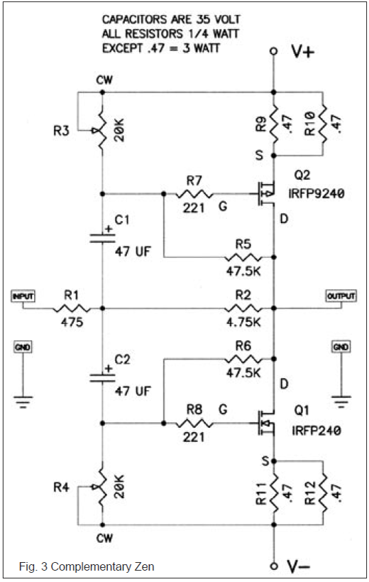
Figure 2 will work just fine as is, but it’s usually more convenient to add some little touches for extra stability. Figure 3 shows a more detailed schematic designed to make life easier for those of you fearless enough to build this amplifier (and I certainly hope you do). First off, we never use Mosfets without some resistance in series with the Gate pins, else they might just fly away with parasitic high frequency oscillation all by themselves, and so we have R7 and R8 to damp out that possibility. The value is not at all critical - somewhere between 100 and 500 ohms will do the job.
Also, you will notice that we have added Source pin power resistors to Q1 and Q2. These help stabilize the DC bias a bit, and also give us
convenient spots across which we can measure the current flow through the circuit. In this case, I have chosen two parallel .47 ohm 3 watt resistors to form a 6 watt .235 ohm resistor (because the Digikey catalog only offers the inexpensive metal film Panasonic power resistors down to .47 ohms). Like the Gate resistors, a wide range of values will work fine.
I suggest between .1 and .5 ohm, keeping in mind that they should be able to handle as much as 4 amps without overheating. All the rest of the resistors will be happy at .25 watt ratings, and none of them are critical in value except R3 and R4.
In a real amplifier, R3 and R4 assume critical values, as they
sensitively control the bias current through the amplifier. We want this bias current to be in a welldefined range, as it bears strongly upon the performance and also the heat dissipation of the circuit. Too little bias current gives high distortion, and too much will cook the transistors. As a consequence, R3 and R4 are adjustable resistors (potentiometers) which will be used to set up the bias current exactly when the finished amplifier is first tested.
Note in Figure 3 that C1 and C2 have now assumed some values and are polarized electrolytic type capacitors. I have no objection to film type capacitors, nor is there any reason not to bypass the 47 uF electrolytic caps with your favorite lower value film types. C1 and C2 should be rated at least the value of the supply voltage, and I recommend 35 volts minimum for this project.
Q1 and Q2 are not particularly critical as to type. I use IRFP240 and IRFP9240 as they work fine, are commonly available and not too expensive. Many other types will work fine. Matching of Q1 and Q2 is not important. The heat sinking for Q1 and Q2 will be an important issue, as we intend to run them between 30 and 75 watts each, depending on the supply and bias. This is somewhat higher than we have seen in the other Zen projects, and even more effort will have to go into keeping these devices at reliable temperatures. In general, we can accept 50 to 60 degrees C. on the heat sink near the transistor mounting point.
The circuit of Figure 3 is quite sensitive to power supply noise
and fluctuation. V+ and V- will need to be stable and quiet, otherwise the bias will wander and noise will appear at the output of the amplifier.
Performance Anxiety
We built up two separate channels of the circuit of Figure 3 and ran a series of bench tests, measuring characteristics at different supply voltages and bias points.
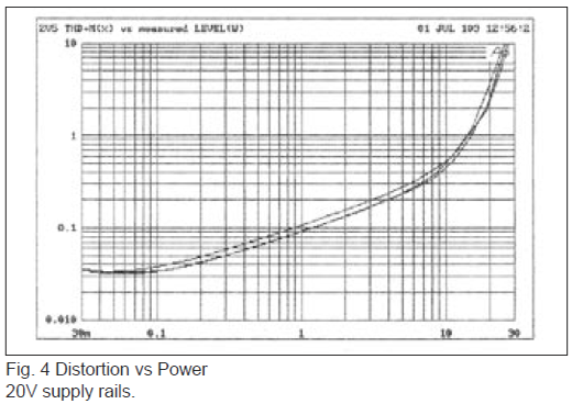
Figure 4 shows the Total Harmonic Distortion and Noise (THD+N) for the amplifier, measured at 1 KHz and driving 8 ohms. The regulated supply voltages V+ and V- have been set at 20 volts each, and three separate curves have been run, showing THD+N versus output power in watts for bias currents of 1.5 amps, 2.0 amps, and 2.5 amps. These bias figures create heat dissipation for each device at about 30 watts, 40 watts, and 50 watts, respectively.
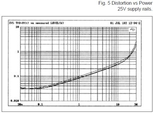
Figure 5 shows the THD+N for the amplifier with the regulated supply voltages V+ and V- at 25 volts each and bias currents of 1.5 amps, 2.0 amps, and 2.5 amps, dissipating about 37 watts, 50 watts, and 62 watts, respectively for each transistor.
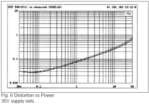
In Figure 6 we see the same test, but with the supply voltages raised to +/- 30 volts, and the dissipation at about 45 watts, 60 watts, and 75 watts for each transistor.
From these curves we find performance that is roughly similar
to the Zen Variations 2 project, with a bit more distortion but also a bit more power. There is not a lot of variation in performance between 1.5 amp, 2.0 amp and 2.5 amp bias, although the higher bias tends to sound better and is also better with low impedance loads. Bias at only 1.0 amp gave much higher distortion under all conditions, and so 1.5 amps is the minimum recommended bias current.
The harmonic character of distortion is primarily second harmonic at lower wattages, in
spite of this being a complementary circuit, and reflects the imprecise matching of the complementary devices. Because the devices are slightly different in gain variations, asymmetry appears in the distortion waveform, creating even order harmonics. At power levels above a couple watts, third harmonic and other odd harmonic components start to dominate, and of course at some point the circuit simply clips pretty much like any other amp.
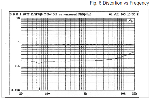
Figure 7 shows the THD plus noise from 20 Hz to 20 KHz measured at 1 watt and without filtering. The distortion climbs at the highest frequencies and is essentially doubled at 20 KHz. The frequency response was measured as – 3dB at about 10 Hz and 100,000 Hz.
The output impedance of the amplifier is relatively high, approximately 2 ohms, giving a damping factor of about 4. This is gain dependent, and improves inversely with gain, so that a higher value of R1 proportionately increases the damping factor.
Quiet, Please
The ZV5 is much more sensitive to supply noise than other amplifiers, and this is because the input AC signal is referenced not to ground, but to the AC value of the supply rails. To the extent that the supply ripple noise is symmetric, there is some cancellation, but what remains is still amplified by the gain of the amplifier. Typically you will find that the value of the noise on the supply is comparable to the noise that appears at the output.
This means that the Complementary Zen requires
very quiet supply. Given a quiet supply however, the noise figures are astonishingly good on our samples; on the order of 18 uV over the audio band. As a rule, commercial manufacturers are happy with 10 times that amount.
Providing the appropriate supply for this circuit is an exercise in big hardware. Usually when we say this we mean big transformers, capacitors and heat sinks, but in this case we mostly mean big capacitors.
Alternatively, you could design an active supply using switching, feedback and other techniques to get the appropriate voltage and current at the noise levels you want. What you want is a source impedance around .05 ohms or less and noise around 10 uV or less. I leave this approach as an exercise for the reader; in this article we are going to do it the big dumb way.
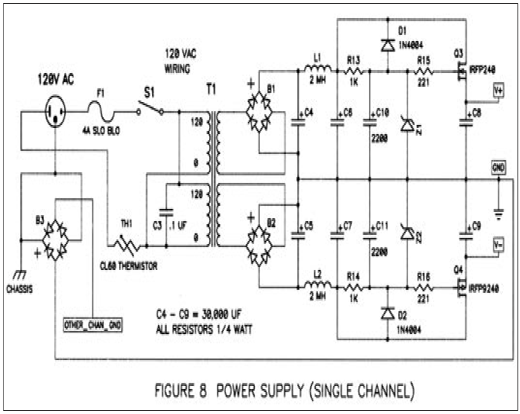
Figure 8 shows the schematic of such a power supply. In many ways this is typical of the power supplies for the Zen amps, but it uses all the tricks to get low noise and low source impedance. Big as it is, this supply is meant for one channel only, as any signal impressed on the supply by one channel will show up on the other channel.
Primary School
Because the design of this circuit is flexible enough to take advantage of a range of supply levels, we cannot specify a particular transformer, and so we will go through a quick exercise to determine what we need.
The power transformer will need to have the voltage and current rating appropriate to the draw of the circuit. In general, you should use a transformer whose VA rating is more than twice that of the circuit draw.
The rule-of-thumb formula for the selection of the transformer is as follows:
VA rating (watts) = 2.5 * 2 * (regulated voltage + 8) * bias current
For the example of +/- 20 volts at 1.5 amps (the smallest example) we get:
For the example of +/- 30 volts at 2.5 amps (the largest example):
VA = 2.5 * 2 * (20 + 8) * 1.5 = 210 watts
For the example of +/- 30 volts at 2.5 amps (the largest example):
VA = 2.5 * 2 * (30 + 8) * 2.5 = 475 watts
Remember, this is per each channel!
Secondary School
We want the unregulated supply coming off bridge rectifiers B1 and B2 to be about 8 volts higher than the desired regulated supply, and that is why you see the number 8 added to the regulated voltage in the above calculation. Of this 8 volts, about a volt will be lost to ripple, about a volt will be lost to DC across the inductors L1 or L2, about 4 volts will be lost from the Gate to Source of regulator transistors Q3 and Q4, and the 2 volts left over will be needed to run a couple of milliamps current through R13 and R14 to drive the Zener diodes Z1 and Z2.
A simple way to calculate the secondary voltages required is to start with the regulated rail voltage, add the 8 volts, add another 3 volts for Bridge and Thermistor losses, and divide by 1.4, which will give you the AC voltage rating of each secondary winding. For the 20 Volt example, we have (20 + 8 + 3) / 1.4 which gives 22 V AC. This figure should be under load, in other words this transformer should deliver this secondary voltage while operated at 200 watts. If a 10% regulation figure is called out on the transformer specs, then consider adding 10% to that 22 V AC. When in doubt, buy a heavier transformer with a bigger VA rating.
You may not get exactly the voltage that you want, but this is not likely to be a real problem. You may have to adjust your expectations for the voltage rating of the Zener diodes Z1 and Z2 to be about 2 volts less than the voltage appearing at the Drains of Q3 and Q4, and everything will probably be fine. If you want the difference voltage to be other than the 2 volts, adjust R13 and R14 so that the current flowing through them to the Zener diodes is about 2 mA.
Fuse F1 is standard Slow Blow type rated at 4 amps or so (for 120V operation). If this proves to be too small, then try 5 amps. If you are running 240 VAC line power, then you will want to halve that figure, as well as running the transformer primary coils in series rather than parallel.
S1 should be a nice big high current rated switch. While it’s true that thermistor TH1 will help reduce large turn-on current surges, the
rating of the switch should be at 25 amps and 250 volts or better. Thermistor TH1 is a Keystone CL60 type, rated at 5 amps steady state current. Of course you can leave both the switch and/or the thermistor out if you wish, they are not truly required for operation.
C3 should be a line-rated capacitor, designed to sit across an AC power line in safety. You can leave it out also, if you wish.
B3 is a power diode bridge, and can be rated the same as B1 and B2, which are 35 amp at 200 volts or so. B1 and B2 clearly have the function of rectifying the secondary AC voltage into the unregulated rails. Some of you will wish to explore the variety of higher-end types of diodes that are available for this purpose, and of course you are encouraged to do so. The prototype was built with big dumb cheap rectifier bridges with no pretension whatsoever.
In the case of B3, the function is to provide a connection to Earth
ground (the one provided by your AC outlet) with a small voltage barrier to prevent the everpresent ground loop that haunts many systems. If your internal ground starts exceeding about .6 volts above Earth ground, B3 will conduct it off to Earth, hopefully keeping you safe from shock in case of transformer failure or some other mishap which makes the ground more lively than is wanted. There are other approaches, and perhaps you can bypass B3 altogether without picking up noise, but for safety reasons you should never disable the Earth ground connection of your system. You will note in Figure 8 that provision is made on B3 for connection to the ground of another channel sharing the same chassis. If there is no other channel sharing the same chassis, you can leave this pin unconnected, or better yet, attach it to the same circuit ground as the other pin.
Capacitors C4 through C8 are rated at about 30,000 uF (or more!) at a voltage exceeding
the unregulated rail voltage (remember: regulated voltage + 8 volts). You cannot skimp too much on these capacitance values and still get a sufficiently quiet supply for this amplifier. You can parallel smaller values if you like, and of course you can add the always popular film capacitors for additional bypass.
Regulation Rules
The Mosfet regulators in this circuit are simply followers, driven by the voltage appearing at their Gates. On a long term DC basis this is determined by the value of the Zener diodes, but fairly large capacitors C10 and C11 are provided not only to help filter noise, but to provide a very slow startup voltage. ZV5 can draw quite a bit of extra current if awakened rapidly due to C1 and C2, and so the 2200 uF values for C10 and C11 give it a gentle wakeup call.
You might imagine that large
capacitance would not be needed coming off the output of the Mosfet regulators, but in fact they are. Q3 and Q4 are operated without feedback, and their intrinsic “resistance” (the inverse of their transconductance) is about .25 ohms, enough to create some undesirable modulation at AC frequencies. This is squashed by the 30,000 uF of C8 and C9 so that it doesn’t become an issue until down about 10 Hz or so, and by then your woofer has much bigger problems than the amplifier.
We note that Zener diodes Z1 and Z2 are chosen to be 4 volts higher than the regulated voltage desired. The appropriate voltages can be formed by placing Zener diodes in series, but the dissipation experienced by each diode should be considered. Typically, each Zener diode will have about 2 mA current running through it, and this multiplied by the Zener voltage forms the dissipation figure. For example, a 34 volt Zener with 2 mA current dissipates 78 mW (.078 watts). A nice .5 watt Zener diode would do well here, and would be unlikely to break.
Diode D1 and D2 are provided to drain off C10 and C11 quickly when the power is turned off, else the 20 Volt Gate to Source ratings of Q3 and Q4 might be exceeded.
The particular characteristics of L1 and L2 are not very important. They simply need to hold about 2 mH of inductance at a DC current up to 3 amps or so without saturating or burning up. Your standard big coil with fat wire will do the job, and remember not to locate it near the amplifier’s input. If fact, with the exception of C8 and C9, the power supply in general is
best kept at a distance from the audio portion of the circuit. No need to get carried away, a foot or so usually does the trick.
Bias Choices
In previous Zen projects we have tended to limit the dissipation on the gain devices to around 25 watts or so, but in ZV5 we are clearly playing a bolder game, with dissipation figures as high as 75 watts per device.
The distortion curves of figures 4, 5 and 6 clearly show that there is not a big difference in distortion versus bias figure between 1.5 amps and 2.5 amps, as the curves tend to cluster together for these figures.
It’s true that in general the sound does get better with the higher bias figures, but the heat to be removed climbs proportionately, and keeping these devices as cool as possible becomes critical when you start exceeding 25 watts or so dissipation.
Let’s just say it outright: There’s no such thing as too much heat sinking. Whatever you think will do the job, go ahead and double it. Your friends and neighbors (if not your wife) will stand in awe of your massive heat sinks, and probably your transistors will survive a few years.
And if you find that you underestimated your heat sinks, don’t despair; any kind of fan blowing air across the sinks will work wonders.
Construction Tips
This is a relatively simple circuit and can easily be built with pointto- point wiring. We will be offering a circuit board and maybe some parts for sale at www.passdiy.com and there is very little else that can’t be obtained from Digikey and similar suppliers.
As always, Mosfets are sensitive to static electricity, and should be handled with some care until they are soldered into the circuit. The gain devices need to be mounted to the heat sink with some care, as the wattage is higher than usual for these projects, and we want to remove as much heat as we can from the chip. Remember that the metal of the transistor cases are Drain connected, and unless you have made special arrangements, they must be electrically insulated using Silicone material or Mica and thermal grease. If you can devote an electrically isolated heat sink to just Q1 and Q2, you can dispense with the insulator, as the circuit connects the Drains of Q1 and Q2 anyway, and just use thermal grease (The computer geeks love Arctic Silver).
Virtually none of the parts in this circuit is critical in value, with the exception of R3 and R4, which are adjustable. Take care in the selection of potentiometers for R3 and R4, since an open wiper on either of them will result in high current and probable failure. If you get to the point where you can precisely replace R3 and R4 with fixed resistors, feel free to do so. Outside of R3 and R4, feel free to alter the values of the parts or use what you happen to have on hand.
Similarly, a large variety of complementary Mosfet parts will work perfectly well. Don’t be afraid to try them out. Watch out for the wattage ratings, and by this I mean never run a part higher than half of its power rating.
You may find that in rare cases the Vgs figure is different enough to require a higher potentiometer range than the 20 Kohm of R3 and R4, but this is unlikely.
Start Me Up!
At this point, assuming that you have carefully constructed this circuit, checked everything twice and then again the next day, it’s time to fire it up.
First, the values of R3 and R4 should be set to the counterclockwise (minimum resistance) setting. Don’t assume anything; check it with an ohmmeter, because if anything will kill this amplifier it will be R3 and R4 set at maximum resistance.
Ideally it is nice to start an amplifier up with a full range of test equipment, monitoring all the voltages and currents, analyzing the distortion and temperature and all that. I like to keep about eight multimeters, three oscilloscopes, an Audio Precision System 1, four soldering irons and a fire extinguisher on my bench. However, I’m going to suggest that you can do this one with a single Radio Shack voltmeter with a DC scale that goes from 1 mV to 100 volts. Also it will be helpful to have some kind of load; some power resistor or perhaps an old disposable dinky speaker (like the crummy one that came with your
computer). We aren’t planning on sending any real power through it; we just find that adjustment goes faster with any kind of load.
You can fully adjust the amplifier by alternately measuring the voltage across two points: Output to Ground, and across the parallel R9/R10 resistors (going from the Source of Q2 to the positive regulated supply). The voltage across the R9/R10 will tell you how much current is going through the transistor Q2, and the voltage at the output to ground will tell you when Q1 is operating at the same current.
Start out with the DC voltmeter on the 2 volt scale, and attach the probes across R9/R10. Turn the AC power on, and stand back. After there is no explosion or fire, check to see that the voltage read by the voltmeter is 0 or maybe only a millivolt or so. If this is the case, now check to see what the voltage at the output to ground is. It also should be quite low, 0 to a few millivolts.
If these voltages are 0 and the fuse hasn’t blown, then we are halfway home. Check the unregulated and regulated supply voltages and confirm that you really did turn the amplifier on. Confirm that there is about 2 volts across R13 and R14 and the voltages across Z1 and Z2 and that the regulated supply voltages are about 4 volts less than the measured Zener voltages. It takes a little while for C10 and C11 to charge, so don’t get excited if these voltages take 10 or 20 seconds to settle in.
Go back to R9/R10 and begin turning R3 clockwise slowly until a few millivolts DC appears across
R9/R10. Then, looking at the DC voltage from output to ground, turn R4 clockwise slowly until the voltage goes from some millivolts positive to about the same number of millivolts negative.
Repeat this procedure, increasing the value of R3 slightly while measuring the DC across R9/R10 and then increasing the value of R4 while measuring the DC output voltage.
Ultimately, you will want to arrive at some stable DC voltages across R9/R10 while also having an output voltage near 0. Assuming that you have chosen R9 and R10 as .47 ohms each, the following voltages will correspond to the desired range of bias current:
353 mV = 1.5 amps
470 mV = 2.0 amps
588 mV = 2.5 amps
As the amplifier warms up, you will want to trim these values, alternately adjusting for the voltage across R9/R10 and then for 0 DC volts at the output. This procedure could take a half hour, maybe more, to get just right. How much output offset voltage is too much? More than 100 mV, in my personal opinion. As a rule, you should be able to get this circuit stable within 50 mV after warmup.
Conclusion
This is a very good sounding amp. It sounds most like ZV2, but with a bit more power and a little more punch on the bottom. Whether it is actually better or not is a matter of taste. At higher bias currents, it definitely delivers more into lower impedance loads. As of this writing
I’m driving a set of Jordan 92’s mounted into rear loaded horns (the upcoming J-Horn project). I believe I could live with this for a couple of years.
Epilogue
As always, many thanks to Karen Douglass and Desmond Harrington for their valuable help, and Sponge Bob Squarepants for inspiration.
“Ohhhhhhh, Who lives in a pineapple under the sea?…….”


