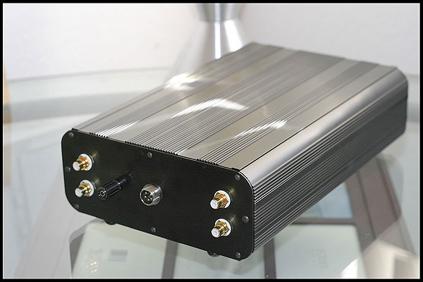
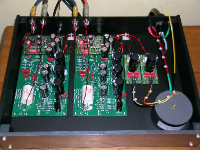
Here is the long awaited sequel to the Pearl phono stage, named after my maternal Grandmother who was good with a sling shot , played piano and organ and occasionally listened to my early Hi-fi efforts if the smoke wasn't too bad. Pearl II addresses the major request received over the years - more gain for moving coil cartridges.
Phono stage design is difficult to do well. Everything matters. Any low level phenomenon occurring in the parts of a phono stage shows up greatly amplified at the loudspeaker. This phono stage has about 55 dB gain at 1 Khz, and another 20 dB at 20 Hz, and when you add 10 dB or so on a line stage preamp and another 30 dB with a power amp you end up with 115 dB of voltage gain, which is getting up toward a million to 1.
The problems are different than for power amplifiers – problems due to resistor noise, semiconductor noise, capacitor noise, contact noise, stray fields, little bits of hysteresis, radio frequencies, all competing with the audio signal in greater proportion. Circuit topology, choice of components, board layout, regulation, and shielding become more crucial to preserving audio quality.
The Circuit
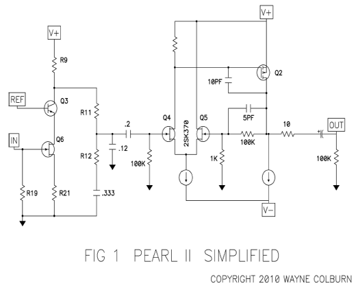
Figure 1 shows the simplified schematic of the Pearl II.
The input signal from the cartridge appears at the Gate of low noise Jfet Q6, which produces a variation in current through Q6. This current variation is fed to the emitter of transistor Q3 which operates in Common-Base mode, forming a cascode connection for Q6. Cascode transistor Q3 does not significantly contribute its own characteristic, nor does it add much to the gain – it is used to shield the Drain of Q6 from the output voltage consequences of the input signal, lowering distortion and improving high frequency bandwidth. The operating point (bias) of Q6 is self setting by the depletion mode character of the Jfet, and Q3 biased by a constant low noise DC voltage derived from the DC power supply. The resulting gain is approximately 35 dB.
The output voltage for this initial stage appears at the collector of Q3, where it drives a passive RIAA equalization network. The result of this equalization appears at the Gate of Q4, the input Jfet of the second gain stage. This stage has a flat gain response of 40 dB. Differential input pair Q4 and Q5 are biased by a constant current source from the negative supply rail, and they drive the Gate of P channel Mosfet Q2, also biased by a constant current source.
Like the first Pearl, the input stage inverts the phase of the signal. Unlike the first Pearl, the second stage is non-inverting, with the result that the output of the phono stage inverts phase. If you care about absolute phase, some accommodation must be made in the system to see to it that the absolute phase at the loudspeakers is correct. If none of your other circuits inverts, then you would need to either reverse the speaker leads or the cartridge leads.
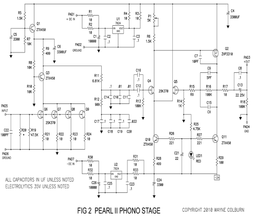
Figure 2 shows the complete schematic.
Here you see the additional details that actually make it work. The raw power supply voltages are regulated by U1 and U2 and their associated circuitry. The unregulated 26 to 35 volt rails are RC filtered, actively regulated down to 24 volts, and then passively filtered again before reaching the rails of the second gain stage. The first (input) gain stage is additionally filtered actively by Q1 and passively by C6 to remove that last tiny bit of noise.
R20 is a user provided resistor value that sets the input load for the cartridge if not the default 47 Kohm. Q6 through 9 are matched parallel Jfets making up the input stage. Paralleling these makes for higher bias current with lower distortion and also lowers the noise by about 6 dB over that of a single device. The RIAA equalization circuit also uses parallel capacitors to get the desired precision values.
The full schematic shows the details of the constant current sources of the second gain stage which uses a red LED to provide the 1.7 volt DC reference driving Q10 and Q11. This means that the current will be set by the values of R26 (1V / 499 Ohm = 2 mA) and R29 (1V / 100 ohm = 10 mA). C7 and C9 provide frequency compensation.
Potentiometer P1 is used to adjust the DC offset at the output on R17.
The overall gain of the circuit as shown is 55 dB @ 1K Hz. Decreasing R14 from 1K to 300 Ohms gives 10 dB more gain when desired for lower output cartridges. R15 which normally would be shorted to 0 ohms can be replaced by a resistor to provide more gain as an alternative to reducing the value of R14. C15 has been placed on the board to allow for additional adjustment of equalization. In both cases these values are up to you.
Measured Performance
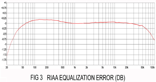
Figure 3 shows the response deviation from ideal RIAA specification.
The curve comes in about plus or minus an eighth of a decibel from 50 Hz to 20 Khz, and reflects my decision to provide subsonic rolloff. You can increase the value of C12 if you would like more bottom end.
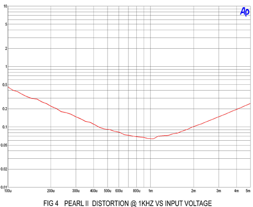
Figure 4 shows the distortion at 1 Khz versus input voltage:
Below about 1 mV input, the distortion continues to decline monotonically, and the curve begins showing the relative proportion of noise below that level.
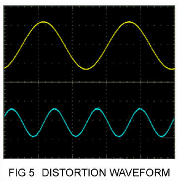
Figure 5 shows the 2ndnd harmonic character of the distortion characteristic, reflecting the single-ended Class A nature of the circuit. This picture was taken at 1 Khz with an input of 3 mV.
Construction
To make it easier for you to build this preamp, we are offering a pc board plus low noise matched Jfets at www.passdiy.com. We supply these items because they would otherwise be difficult to get. The board is unique, and the Jfets have been discontinued by Toshiba. Everything else you should be able to obtain through distributors such as Digikey and Mouser.
There are of course other suppliers, and in the case of the Jfets you can substitute other parts, including 2SK170 and the Linear Devices LSK170 replacements.
Everyone seems to have their own favorite resistors and capacitors. There is nothing particularly magical about these parts – they just work well and are commonly available. You should feel free to play with whatever special components appeal to you.
I used mostly RN55D Dale (Vishay) resistors and a number of Wima polypropylene capacitors, and you will have no difficulty finding more exotic and expensive types.
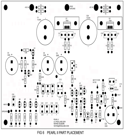
Figure 6 shows the component placement for the circuit board. Please note that this pc board is for one channel.
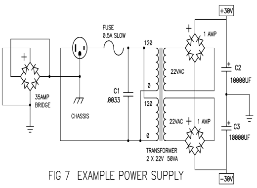
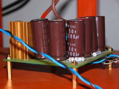
Figure 7 shows an example of the power supply circuit. This is by no means the only way to do it, so feel free to substitute any reasonable supply that delivers the required voltages (28 to 34 volts at 100 mA). You may also elect to use switching supplies, wall-warts, stacked batteries – whatever safely does the job. This supply is designed to work with both channels.
Here we see the usual components found in a DIY linear power supply, with a couple items which directly address the needs of this project. First, there are two rectifier bridges instead of the usual one. We do this because the positive rail will be sourcing more current to the circuit than the negative, and in this circumstance dual rectifiers will avoid the transformer noise which often accompanies this. Also we see that the chassis is directly (and with heavy wire) attached to the earth ground of the AC line and that the signal ground of the circuit is attached to chassis through a high current bridge rectifier as shown.
The bridge is for safety purposes, and we use a standard 35 amp type to ensure that the AC line fuse breaks before the bridge. This avoids ground loops with the rest of the system sharing an AC line ground, while providing an electrical shunt above .7 volts in event of isolation failure. If you find that it lowers the noise, feel free to also connect chassis to circuit ground with a resistor, capacitor, or wire - but leave the bridge in for safety.
35+ volt capacitors are recommended for C2 and C3. C1 is for noise suppression and since it is directly on the AC line it should be specifically line rated.
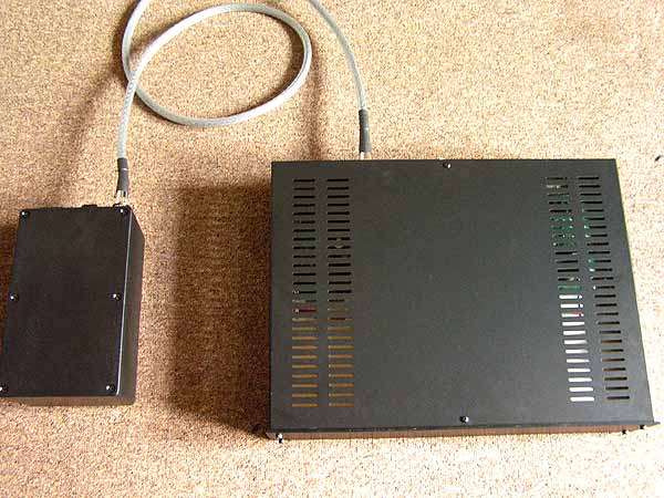
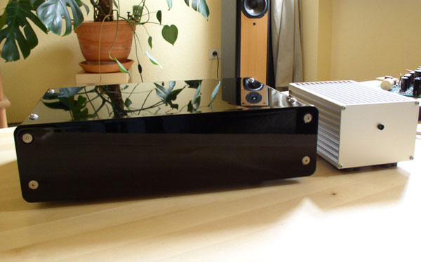
The turntable ground should attach to the signal ground, not the chassis ground (unless you find that it is quieter that way). You probably want to enclose the preamp in a metal chassis to shield it from stray magnetic and radio frequencies. The power supply circuit should be at some distance from the phono stage circuitry, otherwise noise will be picked up. The best approach is usually to put the power supply in a separate enclosure, and if you do this, then Earth ground the power supply enclosure and run just the three wires to the circuit – plus, minus, and circuit ground, grounding the gain stage chassis to signal ground. Don't set the gain stage chassis near the power supply.
Here is the partial Bill of Materials for one channel of the components found on the pc board. Resistors are 0.25 watt
COMPONNENT
VALUE
SOURCE
PART #
C10, 11
01 uF
MOUSER
505-FKP20.01/63/2.5
C13, 21
22 uF/25V
DIGIKEY
604-1052-ND
C10, 11
01 uF
MOUSER
505-FKP20.01/63/2.5
C13, 21
22 uF/25V
DIGIKEY
604-1052-ND
C10, 11
01 uF
MOUSER
505-FKP20.01/63/2.5
C13, 21
22 uF/25V
DIGIKEY
604-1052-ND
C10, 11
01 uF
MOUSER
505-FKP20.01/63/2.5
C13, 21
22 uF/25V
DIGIKEY
604-1052-ND
C10, 11
01 uF
MOUSER
505-FKP20.01/63/2.5
C13, 21
22 uF/25V
DIGIKEY
604-1052-ND
C10, 11
01 uF
MOUSER
505-FKP20.01/63/2.5
C13, 21
22 uF/25V
DIGIKEY
604-1052-ND
C10, 11
01 uF
MOUSER
505-FKP20.01/63/2.5
C13, 21
22 uF/25V
DIGIKEY
604-1052-ND
C10, 11
01 uF
MOUSER
505-FKP20.01/63/2.5
C13, 21
22 uF/25V
DIGIKEY
604-1052-ND
Conclusion
So there we have it. I hope it was worth the wait.
Wayne@passlabs.com
© 2010 Wayne Colburn.
Less...


